Mosaic lateral heterostructures in two-dimensional perovskite
TL;DR
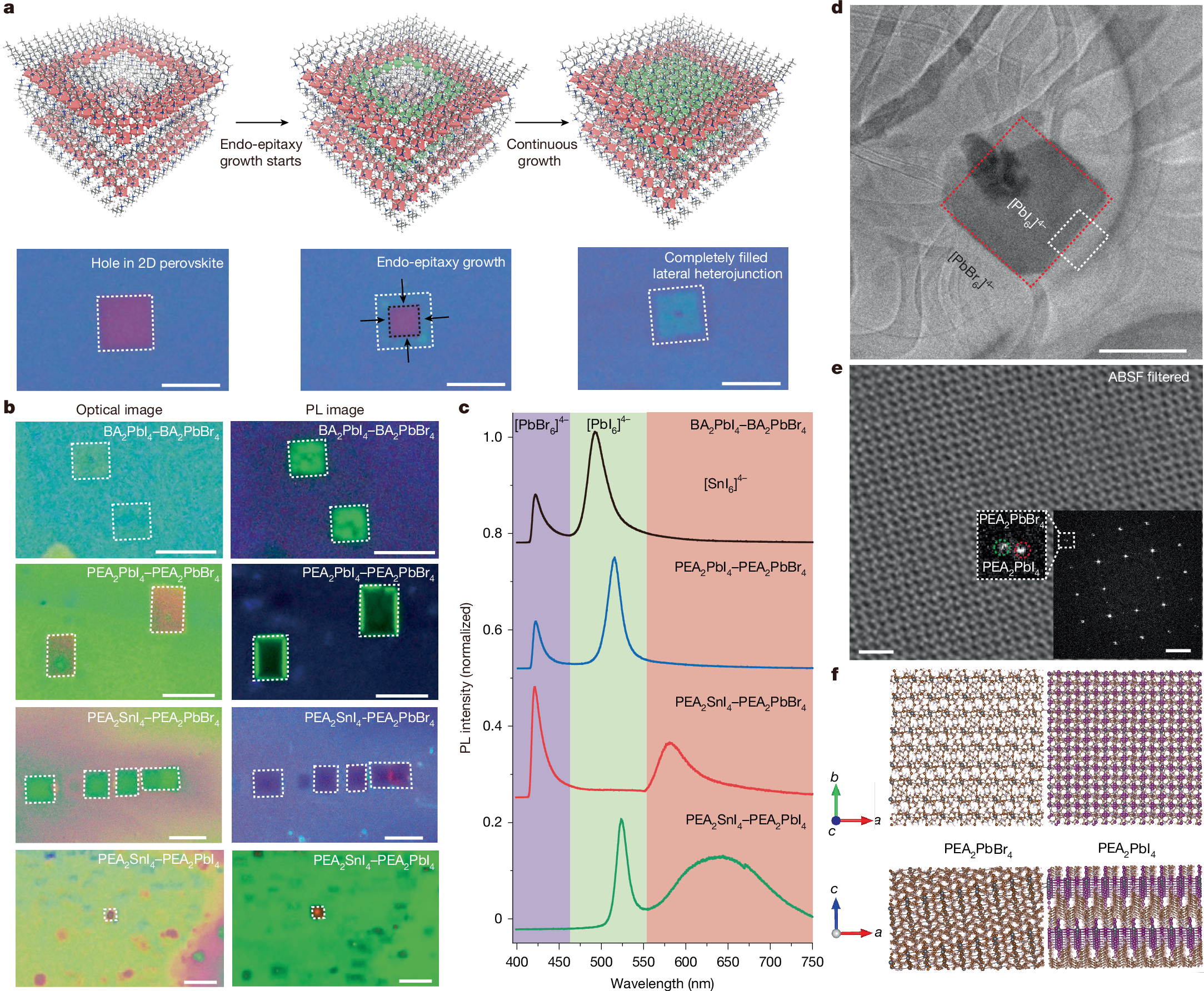
Researchers developed a method to create mosaic lateral heterostructures in 2D perovskites by forming controllable square holes via spontaneous etching and using them as templates for epitaxial growth, enabling multi-color light emission for devices.
Key Takeaways
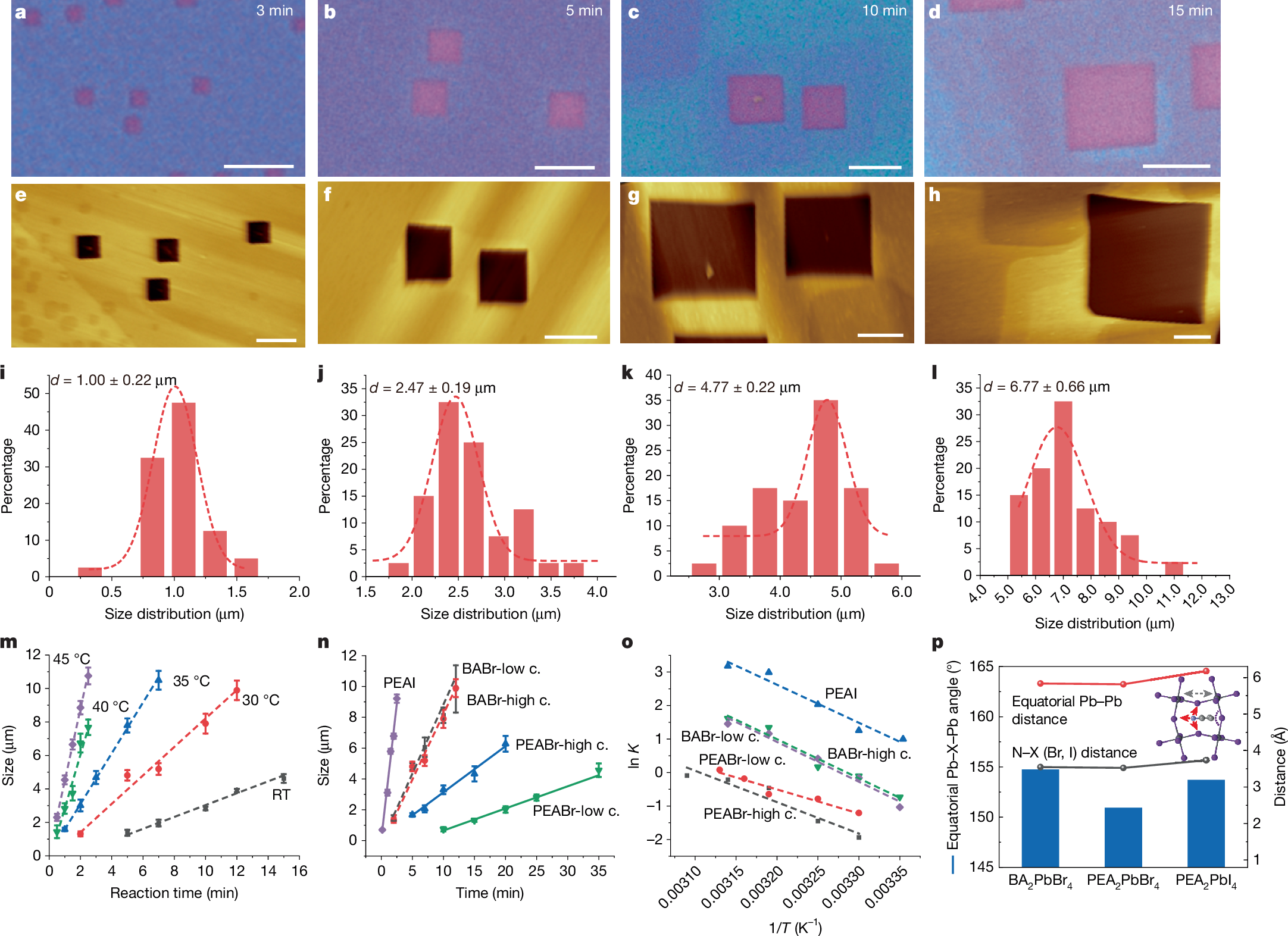
- •Square holes in 2D lead halide perovskites form through spontaneous etching driven by internal strain, with size controlled by etching time and temperature.
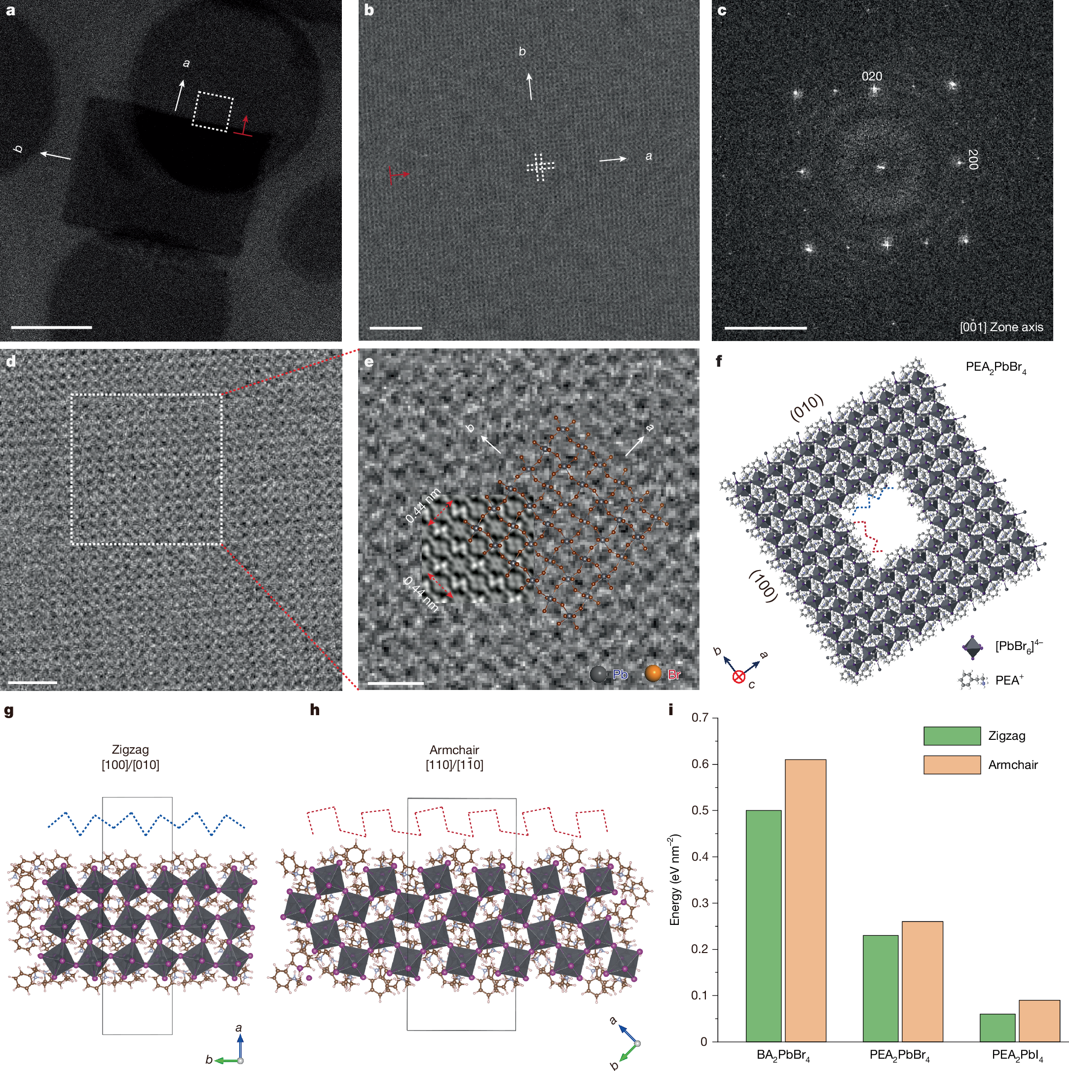
- •The edges of these holes serve as templates for epitaxial growth of different perovskite types, allowing creation of lateral heterostructures.
- •This approach enables fabrication of mosaic heterostructures that emit various colors, useful for light-emitting devices.
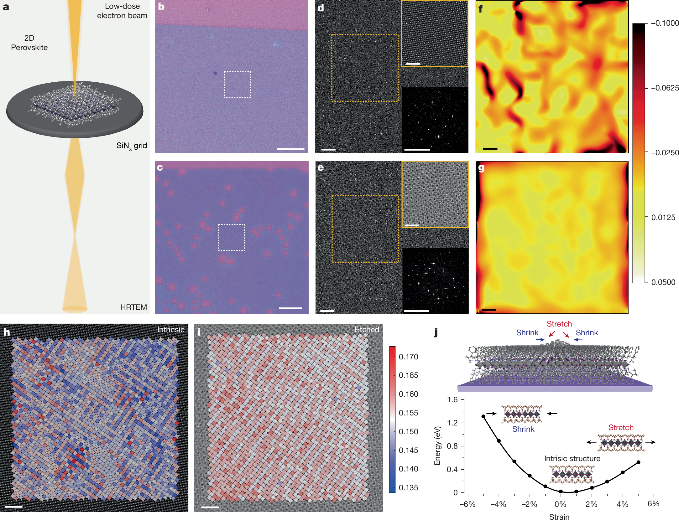
- •The method avoids aggressive lithography and etching, addressing the soft and unstable nature of 2D perovskite ionic lattices.
Tags
Abstract
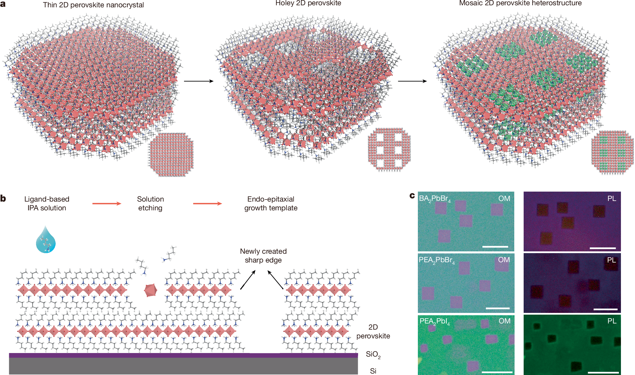
Lateral heterostructures are important for exploring exotic physics, developing new devices and achieving device miniaturization1,2,3,4,5,6,7,8. Endo-epitaxial growth occurring in patterned templates presents a promising strategy to realize extensive patterned areas in heterostructures, as recently demonstrated with two-dimensional (2D) covalent materials9,10,11,12,13. However, the conventional lithography and etching processes used to prepare patterned templates are too aggressive for 2D lead halide perovskites, owing to their inherently soft and unstable ionic lattice14,15,16. Here we create square holes of controllable size within 2D lead halide perovskites, enabling the fabrication of continuous lateral heterostructures over large areas. We demonstrate that the square holes form through spontaneous etching, a process initiated by internal strain and stabilized along the [100]/[010] crystallographic direction. Furthermore, the size of the square holes can be controlled by adjusting the etching time and temperature. Moreover, by incorporating a rapid solvent evaporation growth technique, the edges of the square holes act as templates for epitaxial growth of another type of perovskite, incorporating different halide or metal ions. Finally, we realized a series of mosaic lateral heterostructures that can emit various colours for light-emitting devices. This synthesis of diverse 2D perovskite mosaic lateral heterostructures provides valuable insights into the structural characteristics of perovskites and offers a versatile material platform for the development of complex integrated emitting devices.
Access Nature and 54 other Nature Portfolio journals
Get Nature+, our best-value online-access subscription
$32.99 / 30 days
cancel any time
Subscribe to this journal
Receive 51 print issues and online access
$199.00 per year
only $3.90 per issue
Buy this article
- Purchase on SpringerLink
- Instant access to the full article PDF.
USD 39.95
Prices may be subject to local taxes which are calculated during checkout
Data availability
The data that support the plots in this paper and other findings of this study are available from the corresponding author upon reasonable request. Source data are provided with this paper.
References
Sahoo, P., Memaran, S., Xin, Y., Balicas, L. & Gutiérrez, R. One-pot growth of two-dimensional lateral heterostructures via sequential edge-epitaxy. Nature 553, 63–67 (2018).
Xie, S. et al. Coherent, atomically thin transition-metal dichalcogenide superlattices with engineered strain. Science 359, 1131–1136 (2018).
Li, M.-Y. et al. Epitaxial growth of a monolayer WSe2–MoS2 lateral p–n junction with an atomically sharp interface. Science 349, 524–528 (2015).
Zhang, S. et al. Moiré superlattices in twisted two-dimensional halide perovskites. Nat. Mater. 23, 1222–1229 (2024).
Duan, X. et al. Lateral epitaxial growth of two-dimensional layered semiconduc