Towards fibre-like loss for photonic integration from violet to near-infrared
TL;DR
Researchers developed a CMOS-compatible germano-silicate photonic integrated circuit platform achieving fiber-like ultralow loss from violet to near-infrared wavelengths. The platform demonstrates record-high resonator Q factors exceeding 180 million and enables new applications in optical clocks, quantum sensors, and precision navigation systems.
Key Takeaways
- •Germano-silicate PICs achieve unprecedented ultralow loss (0.08 dB/m at 1064 nm) across violet to telecom wavelengths, representing up to 20 dB improvement over existing platforms.
- •The platform is fully CMOS-foundry-compatible and enables both annealed and anneal-free operation, facilitating heterogeneous integration with temperature-sensitive active components.
- •Key demonstrated capabilities include soliton microcomb generation, stimulated Brillouin lasing, and low-frequency-noise self-injection locking enabled by dispersion engineering, acoustic confinement, and thermal stability.
- •The technology bridges ultralow-loss PICs to critical applications including optical clocks, quantum sensors, precision navigation, and on-chip atom/ion control systems.
Tags
Abstract
Over the past decades, remarkable progress has been made in reducing the loss of photonic integrated circuits (PICs) within the telecom band1,2,3,4, facilitating on-chip applications spanning low-noise optical5 and microwave synthesis6, to lidar7 and photonic artificial intelligence engines8. However, several obstacles arise from the marked increase in material absorption and scattering losses at shorter wavelengths9,10, which prominently elevate power requirements and limit performance in the visible and near-visible spectrum. Here we present an ultralow-loss PIC platform based on germano-silicate—the material underlying the extraordinary performance of optical fibre—but realized by a fully CMOS-foundry-compatible process. These PICs achieve resonator Q factors surpassing 180 million from violet to telecom wavelengths. They also attain a 10-dB higher quality factor without thermal treatment in the telecom band, expanding opportunities for heterogeneous integration with active components11. Other features of this platform include readily engineered waveguide dispersion, acoustic mode confinement and large-mode-area-induced thermal stability—each demonstrated by soliton microcomb generation, stimulated Brillouin lasing and low-frequency-noise self-injection locking, respectively. The success of these germano-silicate PICs can ultimately enable fibre-like loss onto a chip, leading to an additional 20-dB improvement in waveguide loss over the current highest performance photonic platforms. Moreover, the performance abilities demonstrated here bridge ultralow-loss PIC technology to optical clocks12, precision navigation systems13 and quantum sensors14.
Emerging integrated laser technologies in the visible and short near-infrared regimes

Extending the spectrum of fully integrated photonics to submicrometre wavelengths

Lithium tantalate photonic integrated circuits for volume manufacturing
Main
At shorter wavelengths (400–1,100 nm), waveguide losses surge because of two fundamental limitations9,10. First, scattering losses increase as the optical wavelength approaches the scale of surface roughness (surface Rayleigh scattering). Second, absorption losses increase as photon energy enters the Urbach tail of amorphous or crystalline dielectrics. However, many important photonic applications operate in these wavelengths14,15, such as optical clocks, quantum computing and networks, bioimaging, astronomical observation, underwater and data centre communications, compact lidar, and atomic physics studies in general (Fig. 1a). Silica (SiO2) and germanium-doped silica (germano-silicate or Ge-silica) have been widely adopted in optical fibres for short-wavelength operation because of their exceptionally low material absorption16. Nevertheless, because of the need for suspended geometries in the case of silica17,18, or the lack of well-developed fabrication processes for germano-silicate19, the promise of fibre-like loss in a photonic integrated circuit (PIC) platform remains untapped.
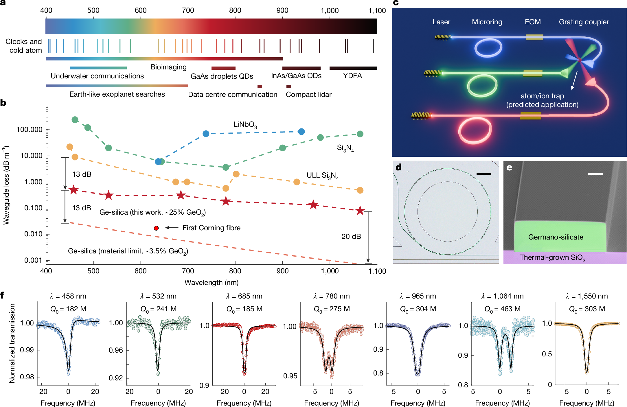
a, Spectrum coverage of photonics application in the visible and short-NIR regions14. QD, quantum dot; YDFA, Yb-doped fibre amplifier. b, Waveguide propagation loss across broadband spectrum of state-of-the-art integrated platforms compared with the present work. Annealed Ge-silica waveguide losses are 0.49 dB m−1 at 458 nm, 0.32 dB m−1 at 532 nm, 0.32 dB m−1 at 685 nm, 0.19 dB m−1 at 780 nm, 0.14 dB m−1 at 965 nm and 0.08 dB m−1 at 1,064 nm, 0.09 dB m−1at 1,550 nm. Unannealed Ge-silica waveguide losses are 1.76 dB m−1 at 458 nm, 1.02 dB m−1 at 532 nm, 0.56 dB m−1 at 685 nm, 0.29 dB m−1 at 780 nm, 0.21 dB m−1 at 965 nm, and 0.19 dB m−1 at 1,064 nm, 0.15 dB m−1 at 1,550 nm. Data from refs. 9,36,37,38 for ULL Si3N4; refs. 10,15,39,40 for Si3N4; refs. 41,42,43 for LiNbO3; ref. 16 for the material limit of Ge-silica (standard modern fibre with a GeO2 content around 3.5 mol%). c, Schematic of high-performance visible PICs with multi-material integration for on-chip atom/ion control, consisting of blocks of III–V lasers, Ge-silica microresonators, LiNbO3 electro-optic modulators and vertical grating couplers. d, Microscopy image of a Ge-silica microring device. e, SEM image of annealed waveguide. f, Transmission spectra and corresponding intrinsic Q factors (Q0) of Ge-silica microring resonators at seven wavelengths spanning from violet to NIR. The observed double-dip features at 780 nm and 1,064 nm arise from mode splitting induced by backscattering in the microcavity, whereas the Fano lineshape at 458 nm originates from multimode interference (see detailed analysis in the Supplementary Information). Scale bars, 500 μm (d); 2 μm (e).
In this work, we present the first step towards using the materials of fibre optics in achieving planar integrated photonic circuits with fibre-like loss. As in fibre optics, GeO2 doping elevates the refractive index of the Ge-silica core, enabling optical confinement within a silica cladding. A deep-ultraviolet (DUV) stepper lithography-based manufacturing process is developed to fabricate planar integrated waveguide circuits on silicon wafers. Leveraging the famously low material loss of Ge-silica16 and the unique low-viscosity reflow properties20 at standard furnace temperatures, we achieve sub-dB m−1 waveguide losses spanning the violet to telecom bands (Fig. 1b). Notably, the waveguide loss in the violet band is 13 dB lower than any current integrated platforms, whereas the lowest loss of 0.08 dB m−1 at 1,064 nm reaches a loss level close to the first low-loss optical fibre produced by Corning in 1970 (0.02 dB m−1) (ref. 21). Crucially, ultralow losses without post-processing thermal annealing can be achieved, which is an important enabler for monolithic/heterogeneous integration with temperature-sensitive materials11.
Beyond its record-low loss performance, several material and practical advantages of this platform are demonstrated. First, the DUV-stepper-defined waveguides are readily dispersion-engineered as required for soliton microcomb generation (demonstrated by soliton microcomb). Second, GeO2 doping reduces the acoustic velocity relative to silica, enabling simultaneous confinement of an optical and acoustic mode within the waveguide core (demonstrated by Brillouin lasing). Finally, it can support thicknesses over 4 μm, enabling low thermorefractive noise (TRN) by the generation of a large mode area (LMA) circuit (demonstrated by low-frequency-noise self-injection locking (SIL)). Overall, this platform incorporates essential ingredients of high-performance multi-functionalized visible PICs, including ultralow loss, multi-material integration ability and high noise suppression, thereby paving the way for high-complexity system-level applications such as on-chip atom and ion control22 (Fig. 1c).
Broadband ultrahigh-Q microresonators
To evaluate performance across the broadband spectrum, microring resonators are fabricated. For this work, air-cladded microring resonators with a 3-mm diameter (corresponding to a 21.2 GHz free spectral range) are used mostly for convenience in coupling and measurement, while also completely eliminating substrate leakage and bending losses (for details, see Supplementary Figs. 1 and 2). The microscopy image of a typical microring resonator is shown in Fig. 1d. The ring and pulley coupler are colorized in green, with ridge waveguides fabricated by etching trenches around the ridges to increase etch efficiency. Unlike Si3N4 photonic circuits, these PICs do not require stress release patterns even at 4 μm of thickness. The inherent low viscosity of Ge-silica can be accessed at standard furnace annealing temperatures, thereby allowing for surface-tension-induced smoothing. By choosing the appropriate temperature, the resonators can achieve atomic-scale smoothness without deformation of the waveguide shape (Fig. 1e). This smoothness overcomes the typical scattering limitations at short wavelengths in integrated microresonators.
U-shape tapered-fibre couplers23 are used to measure Q factors from 458 nm to 1,550 nm. Intrinsic Q factors were determined from transmission spectra scans in the undercoupled regime (for some stronger coupled modes in the visible band, see Supplementary Fig. 5), in which resonant transmitted power and linewidth were used to infer loaded, coupled and intrinsic optical Q factors. A series of tunable external cavity lasers, each calibrated by a separate interferometer, were used to measure Q at each wavelength. Seven resonator transmission spectra at different wavelengths are shown in Fig. 1f, demonstrating intrinsic Q factors exceeding 180 million across a broad wavelength range from 458 nm to 1,550 nm, with the highest Q of 463 million at 1,064 nm, corresponding to a waveguide loss of 0.08 dB m−1. The waveguide loss α is calculated from resonators Q0 by \(\alpha ({\rm{dB}}\,{{\rm{m}}}^{-1})=10\times {\log }_{10}({\rm{e}})\times \frac{2{\rm{\pi }}{n}_{{\rm{eff}}}}{{Q}_{0}\,\lambda }\). Here, neff is the effective index of optical modes and λ is the wavelength. The atomic-scale smoothness, along with the broad ultralow-material-loss window of Ge-silica, enables it to break the short-wavelength limitation and achieve the lowest waveguide propagation losses among all integrated platforms within the visible and short-NIR ranges (Fig. 1b). Notably, the loss at 458 nm is 0.49 dB m−1, which is a 13-dB improvement over previous records.
CMOS-compatible fabrication
The fabrication process for this work is shown in Fig. 2a. In the devices studied, a 4-μm-thickness germano-silica layer (25 mol% GeO2, corresponding to an approximately 2% refractive index difference) is deposited around 270 °C (setting the anneal-free thermal budget for the fabrication flow) by plasma-enhanced chemical vapour deposition (PECVD) on a thick (15 μm) layer of thermal oxide on silicon wafer. The Ge-silica layer is then processed into ridge waveguides through ruthenium (Ru) and silica hard masking24, deep-ultraviolet (DUV) lithography and inductively coupled plasma etching. The Ru mask provides high selectivity in fluorine-based etches enabling high-fidelity deep etching of Ge:silica. To reduce the roughness-induced scattering loss limitation and achieve ultrahigh Q across the broadband spectrum, the entire wafer is subjected to furnace annealing at 1,000 °C for 12–18 h. As shown in Fig. 2b (bottom left), the sidewalls of the Ge-silica waveguides undergo reflow, removing the etch-induced roughness, whereas the thermally grown oxide (THOX) substrate remains unaffected.
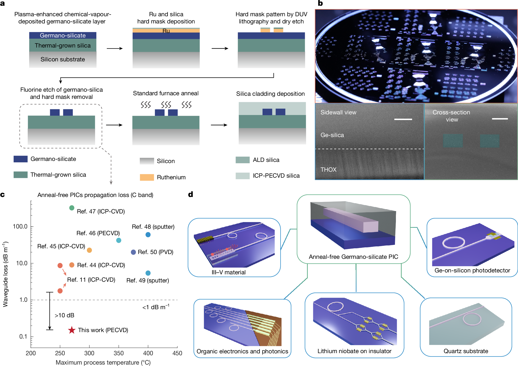
a, Schematic of fabrication workflow for ultrahigh-Q Ge-silica resonators. ALD, atomic layer deposition. b, Photograph of Ge-silica PICs on silicon at wafer scale, SEM image showing the sidewall of an annealed waveguide (intentionally overetched to show the contrast in reflow compared with non-reflowed material) and cross-section of cladded waveguides. c, Anneal-free waveguide loss (C band) compared with temperature for state-of-the-art low-loss PICs11,44,45,46,47,48,49,50 compared with the present work. CVD, chemical vapour deposition; PVD, physical vapour deposition. d, Examples of monolithic/heterogeneous integration applications of ultralow-loss anneal-free Ge-silica PICs, including co-integration with III–V materials, organic electronics/photonics, thin-film lithium niobate, thermal-engineered quartz substrates and Ge-on-silicon photodetectors. Scale bars, 500 nm (b, bottom left); 5 μm (b, bottom right).
From here, an optional upper silica cladding layer can be deposited. Two cladding deposition methods are investigated in this work and applied to different devices. First, a 14-μm thick slightly P-doped (1.5 mol% P2O5) silica cladding is used for full acoustic confinement (Fig. 2b, bottom right). Second, a higher-quality inductively coupled plasma PECVD (ICP-PECVD) is used to protect the devices from contamination and degradation due to long-term atmospheric exposure. With the addition of this ICP-PECVD >6 μm cladding (Extended Data Fig. 2a), the Ge-silica PICs have been confirmed to maintain ultralow loss (optical Q factors >108, as shown in Extended Data Fig. 2b), when exposed to the atmosphere for over several months.
Owing to the high quality of the PECVD Ge-silica layer, high precision of DUV lithography and the well-developed etching process24, the Ge-silica microresonators can achieve ultrahigh Q even before annealing. Air-clad resonators without the reflow smoothing anneal are measured and attain ultrahigh Q of nearly 200 million and maintain ultrahigh Q across a similarly broad spectrum (Extended Data Fig. 1). This corresponds to a lowest waveguide loss of 0.15 dB m−1 at 1,550 nm. Figure 2c compares anneal-free waveguide loss (C band) of state-of-the-art integrated platforms with the present work, which exhibits a more than 10-fold reduction over the previous record. This anneal-free improvement in waveguide loss will enhance the performance of applications requiring co-integration with temperature-sensitive material such as III–V devices, organic electronics/photonics, thin-film lithium niobate, thermal-engineered quartz and Ge-on-silicon photodetectors (Fig. 2d).
Advantages and demonstrations
Beyond the ultralow loss across a broadband spectrum, the Ge-silica PICs have three more key advantages in dispersion engineering, acoustic confinement and thermal noise mitigation. To demonstrate them, soliton microcombs, stimulated Brillouin lasing (SBL) and SIL laser experiments are performed using the new platform. As these applications do not require monolithic or heterogeneous integration with other materials, annealed Ge:silica devices are used.
Single-ring soliton generation
Soliton microcombs represent the main new application area of microcavities and enable transfer of large-scale frequency comb technology to an integrated photonic chip. The Q factor of the microcavity determines the microcomb pumping power required as well as its coherence. However, at this time, the only ultrahigh-Q integrated platform—thin Si3N4—has a limited dispersion-engineering ability because of its thin waveguide thickness. This platform exhibits only normal dispersion and requires coupled-ring structures to generate soliton microcombs25. Here, an integrated Ge-silica resonator is used to demonstrate a new ability for an integrated design: soliton generation in a single ultrahigh-Q microring with anomalous dispersion. The microring resonator was designed to have anomalous dispersion and single-mode transmission as required for soliton generation (Supplementary Figs. 3 and 4). And the soliton mode family dispersion is characterized by measuring the frequency of all modes between 1,520 nm and 1,630 nm using an external cavity laser calibrated by a Mach–Zehnder interferometer (Fig. 3a). There is no observable mode-crossing-induced distortion of the mode family, therefore making the mode family well suited for soliton formation.